Graphics Processing Units (GPUs) have become a cornerstone of modern computing, enabling everything from high-definition gaming to advanced scientific simulations. NVIDIA, one of the leading manufacturers in this space, offers GPUs that are renowned for their performance and innovation. This guide aims to provide a comprehensive overview of NVIDIA GPUs, explaining their architecture, functionality, and the specialized cores that power them.
Section 1: The NVIDIA GPU Architecture
NVIDIA GPUs are architecturally designed to process complex graphics and computational workloads efficiently. This structure can be visualized as a pyramid, with each level representing a different organizational layer. At the top is the grid, which encompasses the entire GPU and its resources.
Graphics Processing Cluster (GPC)
GPCs represent a high-level organizational unit within a GPU. They play a crucial role in workload distribution and resource management across the chip. Each GPC operates relatively independently and includes its own Texture Processing Clusters (TPCs), Streaming Multiprocessors (SMs), and shared resources, ensuring efficient workload distribution and resource management.
The number of GPCs in a GPU varies depending on the model and its intended purpose. High-end GPUs designed for demanding tasks, such as gaming, professional rendering, and complex computational workloads, typically feature more GPCs to handle greater parallel processing demands. In contrast, lower-end GPUs, built for less intensive tasks, have fewer GPCs.
This architectural design allows GPUs to scale performance efficiently according to the requirements of different applications and workloads.
Texture Processing Cluster (TPC)
TPCs handle core graphics workloads that create the visual experiences on our screens. They manage tasks such as:
-
Vertex shading: Transforming 3D vertex coordinates into 2D screen coordinates.
-
Texture mapping: Applying textures (images) to 3D models.
-
Rasterization: Converting polygons into pixels for display.
Each TPC contains multiple SMs, which execute these tasks in parallel. They also include:
-
Texture Units: Handle texture mapping tasks, such as fetching texture data from memory, filtering, and applying textures to pixels or vertices. They ensure textures are mapped correctly onto 3D models to create detailed and realistic images.
-
L1 Cache: A small, fast memory cache that stores frequently accessed texture data and instructions, reducing latency and improving the efficiency of texture processing.
-
Shared Memory: Allows efficient data sharing among the texture units and SMs within the cluster, which is crucial for high-performance texture mapping and filtering operations.
-
Special Function Units (SFUs): Optimized for texture mapping and rendering operations, handling complex mathematical functions required for texture processing.
-
Raster Engine: Converts vector graphics (such as 3D models) into raster images (pixels), playing a crucial role in the final stages of rendering by determining how textures are applied to individual pixels on the screen.
-

-
Texture Caches: Store texture data close to the texture units, minimizing the time required to fetch this data from the main memory and speeding up the texture mapping process by reducing memory access latency.
Streaming Multiprocessors (SMs)
SMs are the fundamental processing units within the GPU. The number of SMs in a GPU significantly impacts its overall performance. For example, the RTX A5000 has 64 SMs, while the NVIDIA H100, optimized for deep learning, has 168 SMs. Here’s a breakdown of SM components:
-
Instruction Cache (I-Cache): Stores instructions for the SM, allowing quick access and reducing latency by keeping frequently used instructions close to the execution units.
-
Multi-Threaded Issue (MT Issue): Manages the dispatch of instructions to various execution units within the SM, handling multiple threads simultaneously to optimize computational resource use.
-
Constant Cache (C-Cache): Stores constant data that doesn’t change during execution, allowing quick access to these values by the threads.

-
Streaming Processors/CUDA Cores (SP): Execute most of the arithmetic operations (e.g., floating-point and integer operations). Multiple SP units enable parallel processing of instructions.
-
Special Function Units (SFU): Handle complex mathematical functions like trigonometric calculations, exponentials, and other special functions that are more computationally intensive than standard arithmetic operations.
-
Double Precision Units (DP): Handle double-precision floating-point operations, essential for applications requiring high numerical precision, such as scientific computations and simulations.
-
Shared Memory: Fast on-chip memory accessible by all threads within an SM allows efficient data sharing and coordination among threads, significantly speeding up computations requiring frequent data exchanges.
-
L1 Cache: A small, fast memory cache that stores frequently accessed data and instructions close to the SM cores to reduce access times.
-
Registers: High-speed storage locations within each SM store temporary data for active threads, allowing rapid access during computations.
-
Tensor Cores: Specialized for deep learning and AI tasks, performing matrix operations essential for training and inference in neural networks.
-
Ray Tracing Cores (RT Cores): Dedicated to handling ray tracing calculations, providing real-time rendering of realistic lighting, shadows, and reflections.
Each SM integrates these components to execute a wide range of parallel processing tasks efficiently, balancing general-purpose computation with specialized processing for graphics, AI, and other demanding workloads.
In the following sections, we will explore the individual components of the SM in more detail, examining how CUDA cores, RT Cores, Tensor Cores, and shared memory work together to deliver the impressive performance that NVIDIA GPUs are known for.
Section 2: CUDA Cores
NVIDIA GPUs harness their remarkable computational power from numerous CUDA cores, which serve as the fundamental units of parallel processing. These cores enable GPUs to excel in tasks that demand significant computational throughput.
Here's a breakdown of the key components within a typical CUDA Core:
-
Integer Unit: Performs arithmetic operations (addition, subtraction, multiplication, division) on integer data types.
-
[Floating-Point Unit (FPU)](https://en.wikipedia.org/wiki/Floating-point_unit#:~:text=A%20floating%2Dpoint%20unit%20(FPU,operations%20on%20floating%2Dpoint%20numbers.): This unit handles arithmetic operations (addition, subtraction, multiplication, division) on floating-point data types, such as single-precision FP32 and half-precision FP16.
Register File: Registers are a small set of high-speed storage locations within the CUDA Core that hold operands (input data) and computation results. They are crucial for fast data access during calculations.
Instruction Decoder: Converts incoming machine code instructions into micro-operations that the ALU can execute.
Controls Execution: Manages instructions and data flow through the CUDA Core, ensuring correct operation sequencing and accurate result storage.
Memory Access: Manages data loading from memory into registers and storing results back to memory, interacting with the GPU's memory hierarchy (shared memory, L1 cache, global memory).

Additional Components (Optional):
-
Special Function Unit (SFU): This unit accelerates specific mathematical functions, such as sine, cosine, exponential, and reciprocal.
-
Branch Unit: Handles conditional branching instructions, enabling the CUDA Core to take different execution paths based on comparison results.
How CUDA Cores Work
The basic unit of execution on a GPU is a thread. Each CUDA core within a Streaming Multiprocessor (SM) can execute one thread simultaneously. Threads are organized into groups of 32 called warps, which are scheduled and executed concurrently on an SM.
Threads can also be grouped into larger units called blocks, which enable cooperation and data sharing among threads. A block is assigned to a single SM, and the threads within that block share resources on the SM, including registers and shared memory. If a block has more threads than the SM has CUDA cores, the threads are divided into warps, and the warps are scheduled for execution as CUDA cores become available.
CUDA cores operate under the Single Instruction, Multiple Threads (SIMT) architecture, meaning that all 32 threads within a warp execute the same instruction in parallel but on different data elements. This maximizes the Single Instruction, Multiple Data (SIMD) parallelism, where a single instruction operates on multiple data points simultaneously, allowing for efficient processing of large workloads.
The GPU's scheduler in the GPC is responsible for assigning warps to available SMs for execution. When a warp encounters a long-latency operation, such as memory access, the scheduler can switch to another ready-to-execute warp, minimizing latency and maximizing throughput. This dynamic scheduling ensures that the GPU's resources are utilized efficiently, even when dealing with tasks with varying execution times.
The CUDA cores in a GPU can range from hundreds to thousands, depending on the GPU model and its intended use case. In addition to the standard CUDA cores, modern NVIDIA GPUs feature specialized cores designed for specific tasks, enhancing the GPU's capabilities. Let's investigate these specialized cores and their roles in boosting GPU performance.
Section 3: Specialized Cores for Ray Tracing and AI
While CUDA cores are fundamental to GPU processing, modern NVIDIA GPUs have introduced specialized cores that significantly enhance performance for specific tasks. The RT Cores and Tensor Cores have revolutionized real-time ray tracing and artificial intelligence applications, pushing the boundaries of graphics and computing.
RT Cores: Enhancing Ray Tracing
Ray tracing is a sophisticated rendering technique that mimics the physical behavior of light to create incredibly realistic images. However, real-time ray tracing has traditionally been challenging due to its computational demands, especially for interactive applications like video games.
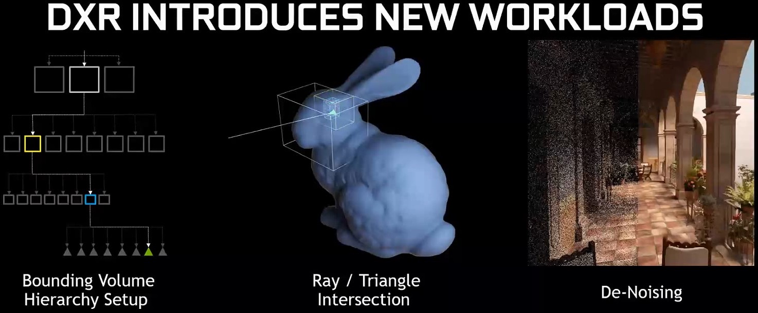
NVIDIA's RT Cores are dedicated hardware units that accelerate ray tracing calculations. They specialize in ray-triangle intersection tests, a critical component of ray-tracing algorithms. By offloading these intensive calculations from the CUDA cores, RT Cores significantly boost the performance and efficiency of ray tracing, enabling real-time, ray-traced graphics in games and other applications.
Key Components of RT Cores:
-
Ray Generation Units: These units generate rays from the camera or light sources, determining the origin and direction of each ray based on scene data and camera parameters.
-
Ray-Triangle Intersection Units: These units perform rapid intersection tests to determine if a ray intersects with a triangle in the scene geometry, a crucial step in ray tracing.
-
[Bounding Volume Hierarchy (BVH) Traversal Units](https://en.wikipedia.org/wiki/Bounding_volume_hierarchy#:~:text=A%20bounding%20volume%20hierarchy%20(BVH,enclosed%20within%20larger%20bounding%20volumes.): These units navigate through BVHs—hierarchical data structures that accelerate ray-object intersection tests. They quickly identify relevant parts of the scene to reduce the number of tests needed.
-
Ray Payload Units: These units manage data associated with each ray, including its origin, direction, and other properties needed for further calculations like shading and material interactions.
Ray Tracing Workflow:
-
Scene Preprocessing: Before ray tracing begins, the scene's geometry is organized into a BVH, typically constructed on the CPU. This structure is crucial for accelerating subsequent intersection tests.
-
Ray Generation: RT Cores initiate the process by generating rays based on camera parameters and scene information.
-
Ray-Scene Intersection Testing: RT Cores use the BVH to determine potential intersections between rays and scene objects, performing both ray-bounding box and ray-triangle intersection tests.
-
Shading: For indirect lighting, RT Cores generate secondary rays to determine how light contributes to the final color of each pixel. They handle complex calculations involving reflections, refractions, and multiple light bounces.
-
Additional Tasks: Depending on the implementation, RT Cores might also handle denoising and global illumination, though CUDA Cores continue to handle tasks like shading calculations and post-processing effects.
Tensor Cores: Accelerating AI and Deep Learning
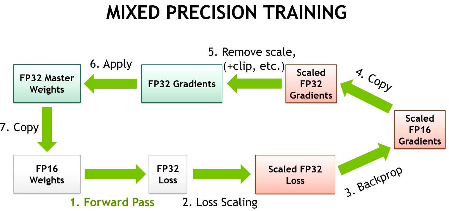
NVIDIA's Tensor Cores are specialized processing units designed to accelerate deep learning operations. They are optimized for matrix multiplications and convolutions—key operations in deep neural networks. Tensor Cores leverage mixed-precision computing, using both single-precision and half-precision floating-point numbers to maximize throughput without compromising accuracy.
Key Components of Tensor Cores:
-
Matrix Multiply-Accumulate (MMA) Units: These units perform 4x4 matrix multiply-accumulate operations in a single clock cycle. Multiple MMA units work in parallel to speed up large matrix operations.
-
Warp Schedulers: These units manage and schedule the execution of warps (groups of threads) on Tensor Cores, ensuring optimal data flow and computation.
-
Registers and Shared Memory: Tensor Cores utilize high-speed registers and shared memory to store intermediate results and data shared among threads.
-
Mixed-Precision Support: Tensor Cores support mixed-precision computing, balancing speed and accuracy by using formats such as FP16, FP32, INT8, and INT4. This flexibility is particularly useful for deep learning models that don’t always need high precision.
Tensor Core Workflow:
-
Input Data Preparation: Input data (e.g., matrices representing images or text) is loaded into GPU memory. It may be converted to lower precision formats to leverage Tensor Cores' mixed-precision capabilities.
-
Matrix Operation Scheduling: The deep learning framework identifies and schedules matrix multiplication and accumulation operations on Tensor Cores.
-
-
Data Fetch: Tensor Cores retrieve the necessary matrix values from GPU memory.
-
Matrix Multiplication: Each Tensor Core performs 4x4 matrix multiplications, producing a result matrix.
-
Accumulation: Results from multiple 4x4 operations are accumulated to compute the final result of larger matrix operations.
-
Output: The final results are stored back in GPU memory.
-
-
Mixed-Precision Handling (Optional): If mixed-precision is used, intermediate results may be computed in FP16 and converted back to FP32 for final accuracy if needed.
-
Iteration and Completion: The process repeats for all scheduled operations until the deep-learning computation is complete.
Tensor Cores have become crucial for accelerating deep learning, enabling the training of more complex models and facilitating breakthroughs in various domains. For instance, they have supported the development of large language models like GPT-3, which excel in generating human-like text, translating languages, and writing code.
Together, RT Cores and Tensor Cores represent a leap forward in GPU technology, driving advancements in both real-time graphics and artificial intelligence.
Section 4: Memory Architecture and Management
Effective memory management is vital for maximizing performance in NVIDIA GPUs. This section explores the complex memory architecture that enables NVIDIA GPUs to process vast amounts of data while minimizing latency and maximizing throughput. We will cover shared memory, L1 cache, L2 cache, GDDR memory, and High Bandwidth Memory (HBM), as well as the roles of memory controllers and interfaces in managing data movement.
Shared Memory

Shared memory is a high-speed, low-latency memory region available to all threads within a thread block. Positioned on-chip within the Streaming Multiprocessor (SM), it facilitates communication and synchronization between threads, enabling efficient data exchange and coordination. Because shared memory is much faster than global memory, it helps reduce latency and improve performance. For instance, in image processing tasks, threads working on adjacent pixels can use shared memory to exchange data, eliminating redundant global memory accesses.
L1 Cache
The L1 cache is a small, high-speed cache located within each SM, designed to store frequently accessed data and instructions. It is typically divided into separate instruction and data caches, allowing simultaneous access to both. By storing frequently used data and instructions, the L1 cache reduces the need to access slower memory levels, such as shared or global memory, thereby decreasing memory access latency and enhancing overall performance. This ensures that CUDA cores remain consistently supplied with data and instructions.
L2 Cache
The L2 cache is a larger, albeit slower, cache shared among all SMs within a Graphics Processing Cluster (GPC). It serves as an intermediary between the L1 cache and global memory, holding data accessed less frequently than L1 cache data but more often than global memory data. By caching data shared across multiple SMs, the L2 cache helps alleviate the performance bottleneck caused by frequent global memory accesses. This reduces contention for global memory bandwidth and improves overall throughput.
GDDR and HBM Memory
Modern NVIDIA GPUs use two primary types of memory: GDDR and High Bandwidth Memory (HBM). Each has distinct characteristics suited to different needs.
GDDR Memory

Graphics Double Data Rate (GDDR) memory is designed for high-speed data transfer in GPUs. It offers substantial bandwidth and low latency, making it ideal for handling large volumes of graphics and compute data. GDDR memory is connected to the GPU via a wide memory interface, allowing parallel data transfers. With advancements like GDDR6, GDDR6X, and GDDR7, the latest generations of GDDR memory provide increased bandwidth and lower power consumption. However, GDDR memory has limitations in maximum achievable bandwidth.
High Bandwidth Memory (HBM)
High Bandwidth Memory (HBM) addresses the bandwidth limitations of GDDR by stacking multiple memory dies vertically and connecting them with through-silicon vias (TSVs). This stacking, combined with a wider interface, delivers significantly higher bandwidth compared to GDDR memory. HBM is ideal for applications requiring rapid data transfer, such as deep learning, scientific simulations, and high-performance computing. Although HBM offers superior performance, its complex 3D structure and TSVs make it more expensive to manufacture.
Why GDDR and HBM Coexist
-
Cost: GDDR is more cost-effective to produce, making it suitable for consumer-grade GPUs where affordability is crucial. HBM, with its intricate design, is more expensive.
-
Power Consumption: GDDR typically consumes more power than HBM, making it less suitable for power-constrained devices like laptops and mobile devices, where HBM's lower power consumption is advantageous.
-
Performance Requirements: While HBM provides superior bandwidth, GDDR can still deliver high performance for many applications, making it suitable for gaming GPUs and other consumer-oriented devices.
Memory Controller and Interface
The memory controller is a key component in GPU architecture, managing data flow between the GPU and the memory (GDDR or HBM). It schedules memory access, ensures data integrity, and optimizes memory bandwidth utilization. The memory interface, comprising multiple data channels, provides the physical connection between the GPU and memory, enabling parallel data transfers to maximize bandwidth.
Understanding the roles of shared memory, L1 and L2 caches, GDDR and HBM memory, and the memory controller and interface provides valuable insights into how data is organized and accessed within NVIDIA GPUs. This knowledge is crucial for optimizing application performance and achieving the best results from GPU-based computations.
Section 5: Display and Output Technologies
For GPUs optimized for video rendering, the final stage in the pipeline involves converting the processed data into a visual output that appears on our screens. This section explores the key components of NVIDIA GPUs responsible for display and output, including the Raster Engine, Raster Operations Pipelines (ROPs), Display Controller, and Video Output Ports. Together, these technologies ensure that rendered images are displayed with high fidelity and seamless performance.
Raster Engine

The Raster Engine is crucial for transforming geometric data (such as polygons and triangles) into a raster image composed of pixels. This process involves determining which pixels are covered by each polygon and assigning the appropriate color and depth values. The Raster Engine performs this task for every frame, ensuring that the final image accurately represents the 3D scene.
Key functions of the Raster Engine include:
-
Triangle Setup: Preparing triangle data for rasterization by calculating edge slopes and determining pixel coverage.
-
Pixel Shading: Computing the final color of each pixel based on lighting, material properties, and other factors.
-
Z-Buffering: Maintaining a depth buffer to identify visible objects and determine which are occluded.
-
Anti-Aliasing: Smoothing jagged edges of polygons to enhance image quality.
Advanced Raster Engines in NVIDIA GPUs are optimized for high throughput, enabling the handling of complex scenes with millions of polygons at impressive frame rates.
Raster Operations Pipelines (ROPs)

Raster Operations Pipelines (ROPs) handle the final stages of pixel processing before the image is output to the screen. Their tasks include:
-
Blending: Combining the colors of overlapping objects to create transparency and other visual effects.
-
Depth Testing: Determining pixel visibility based on depth values.
-
Anti-Aliasing: Further smoothing edges to reduce visual artifacts.
-
Gamma Correction: Adjusting brightness and contrast for optimal display.
-
Display Output Formatting: Preparing pixel data for transmission to the display.
The number of ROPs in a GPU affects its fill rate, which determines how quickly it can render pixels. High-end GPUs with more ROPs handle higher resolutions and more complex scenes with greater ease.
Display Controller
The Display Controller serves as the interface between the GPU and the display device. It processes pixel data from the ROPs and formats it for the display. The Display Controller also manages:
-
Resolution and Refresh Rate Management: Setting display resolution and refresh rate according to user preferences and monitor capabilities.
-
Color Space Conversion: Converting image data from the GPU's color space to the display's color space.
-
Scaling and Rotation: Adjusting image size and orientation to fit the display.
-
Video Output Signal Generation: Creating the appropriate video signal (e.g., DisplayPort, HDMI) for transmission to the display.
Modern Display Controllers support high resolutions, refresh rates, and technologies like G-Sync and High Dynamic Range (HDR), delivering smooth and vibrant visuals.
Video Output Ports
Video Output Ports are the physical connectors on the GPU that interface with display devices. Common ports include:
-
DisplayPort: A high-speed digital interface supporting high resolutions, refresh rates, and features like G-Sync and HDR.
-
HDMI: A widely used interface that supports high resolutions and audio transmission.
-
DVI: An older digital interface still used for some legacy displays.
The variety of video output ports provides flexibility in connecting NVIDIA GPUs to different types of displays, ranging from high-end gaming monitors to large-screen TVs.
In summary, the Raster Engine, ROPs, Display Controller, and Video Output Ports work in unison to transform GPU-generated data into stunning visuals on our screens. Understanding how these components collaborate is key to appreciating the complexity and capability of modern GPU technology.
Section 6: Multi-GPU Systems and Communication
As computing demands escalate, single GPUs may no longer suffice. To address these challenges, NVIDIA has developed technologies to integrate and coordinate multiple GPUs within a system. This section focuses on NVLink, a high-speed interconnect technology that enhances data transfer and collaboration between GPUs, offering significant scalability and performance advantages for various high-performance computing applications.
NVLink: High-Speed Interconnect
NVLink is NVIDIA's high-bandwidth, energy-efficient interconnect technology designed for direct communication between GPUs and, occasionally, between GPUs and CPUs. Unlike traditional PCIe (Peripheral Component Interconnect Express) connections with limited bandwidth and introduced latency, NVLink provides a direct, high-speed data exchange path.
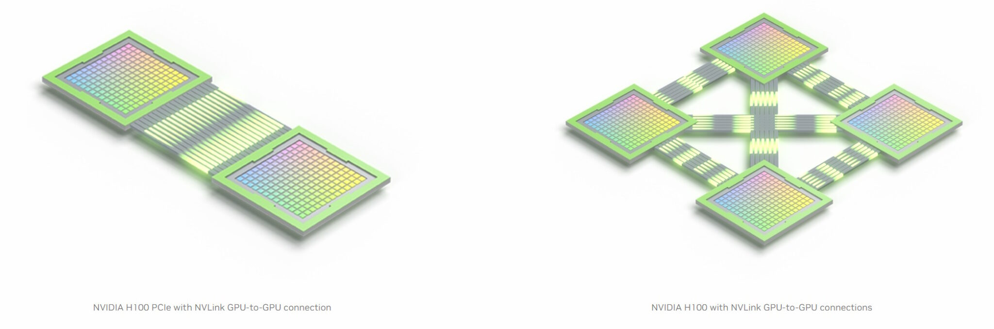
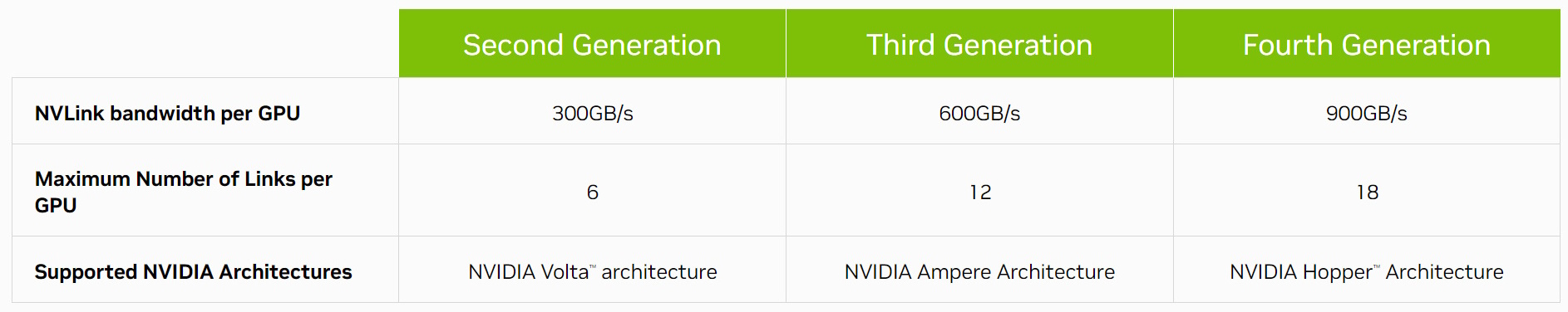
Key features of NVLink include:
-
High Bandwidth: NVLink offers significantly greater bandwidth than PCIe, facilitating rapid data transfers between GPUs.
-
Low Latency: NVLink's direct connections minimize latency, enhancing communication and synchronization between GPUs.
-
Scalability: NVLink supports various multi-GPU configurations (e.g., mesh, ring), offering flexibility for different system setups.
-
Energy Efficiency: NVLink is designed to be energy-efficient, reducing power consumption while delivering high performance.
Scalability and Performance Benefits
NVLink's high bandwidth and low latency enable substantial scalability and performance improvements in multi-GPU systems. By distributing workloads across multiple GPUs and enabling direct communication, NVLink accelerates a wide range of applications, including:
-
Deep Learning: Training and inference of large models are accelerated by leveraging the combined power of multiple GPUs.
-
High-Performance Computing (HPC): Simulations and computational tasks benefit from NVLink's fast data transfer and synchronization.
-
Professional Visualization: Applications like 3D rendering and video editing achieve near-real-time performance with NVLink-enabled GPU clusters.
Applications in High-Performance Computing
NVLink has become integral to high-performance computing, where massive computational power is essential. Data centers and research institutions use NVLink to build powerful multi-GPU clusters capable of tackling complex problems. Notable applications include:
-
Climate Modeling: Accelerating climate simulations for more accurate predictions and understanding of climate change.
-
Drug Discovery: Speeding up the analysis of vast datasets to expedite drug development.
-
Autonomous Vehicles: Enhancing the training and deployment of complex algorithms for safer and more efficient transportation.
NVLink's ability to facilitate seamless communication and collaboration between multiple GPUs is crucial for unlocking the full potential of GPU computing. As computational demands continue to rise, NVLink will play a pivotal role in advancing high-performance computing capabilities.
Conclusion
NVIDIA's GPU technology continues to evolve with each new generation, and the Blackwell series represents the latest advancement. This guide has offered a thorough overview of the core components in modern NVIDIA GPUs, but the Blackwell series introduces additional innovations, such as FP4 precision and other enhancements to existing features.
FP4 precision is a notable advancement that is not covered in detail in this guide. It reduces the bit-width used to represent floating-point numbers, accelerating calculations and decreasing memory requirements. While FP4 precision may compromise some numerical accuracy, it significantly boosts performance for AI inference tasks, where speed often takes precedence over precision.
In practical terms, Blackwell GPUs have the capability to tackle computationally intensive challenges, such as high-fidelity climate simulations performed by Earth-2.